|
 about about
have new idias?
SPM museum
scan-gallery

|
MUSEUM of SCANNING PROBE MICROSCOPY and NANOTECHNOLOGY
The organizers of a Museum beforehand apologize for
incompleteness of an exposition and ask the visitors of a Museum to send the
remarks and exhibits.
Founding Fathers of Scanning Probe Microscopy.
The
founders Scanning Probe Microscopy are Binnig и Rohrer. Patent for
Scanning Tunneling Microscope was issued Aug. 10, 1982 (Priority Sept. 20,
1979)
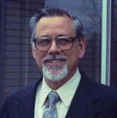
Heinrich Rohrer, left, and
Gerd K. Binnig, right, scientists at IBM's Zurich Research Laboratory in
Switzerland, are awarded the 1986 Nobel Prize in physics for their work in
scanning tunneling microscopy. The researchers are recognized for developing the
powerful microscopy technique, which allows scientists to view individual atoms
on the surface of a sample. The photo is kindly submitted for a museum by Dr. G.
Binnig.
Heinrich Rohrer
Heinrich Rohrer, along with his colleague, Gerd K. Binnig, was awarded
the Nobel Prize in Physics in 1986 for his work in scanning tunneling
microscopy. Binnig and Rohrer were recognized for developing the powerful
microscopy technique, which can form an image of individual atoms on a metal or
semiconductor surface by scanning the tip of a needle overthe surface at a
height of only a few atomic diameters.They shared the award with German
scientist Ernst Ruska, designer of the first electron microscope.
Born
in Buchs, Switzerland, on June 6, 1933, Dr. Rohrer was educated at the Swiss
Federal Institute of Technology in Zurich, where he received his bachelor's
degree in 1955 and his doctorate degree in 1960. After post-doctoral work at the
Swiss Federal Institute and Rutgers University in the United States, Dr. Rohrer
joined IBM's newly formed Zurich Research Laboratory, studying, among other
things, Kondo materials and antiferromagnets before turning his attention to
scanning tunneling microscopy. Dr. Rohrer was appointed an IBM Fellow in 1986,
and was manager of the physical sciences department at the Zurich Research
Laboratory from 1986 to 1988. He retired from IBM in July 1997. Last job -
Laboratory of Physics of small systems and Nanotechnology, Calle Serrano 144 ,
Madrid 28006, Espana. E-mail: h.rohrer@fsp.csic.es
Gerd K. Binnig
Gerd K. Binnig, along with his colleague,
Heinrich Rohrer, was awarded the Nobel Prize in Physics in in
1986 for his work in scanning tunneling microscopy. Binnig and
Rohrer were recognized for developing the powerful microscopy
technique, which can form an image of individual atoms on a
metal or semiconductor surface by scanning the tip of a needle
overthe surface at a height of only a few atomic diameters.
They shared the award with German scientist Ernst Ruska,
designer of the first electron microscope.
Born in Frankfurt, Germany, on July 20,
1947, Dr. Binnig was educated at J.W. Goethe University in
Frankfurt, where he received his bachelor's degree in 1973 and
his doctorate degree in 1978. That year he joined a physics
research group at IBM's Zurich Research Laboratory. Dr. Binnig
was assigned to IBM's Almaden Research Center in San Jose,
Calif., from 1985 to 1986, and was a visiting professor at
nearby Stanford University from 1987 to 1988.
Dr. Binnig was appointed an IBM Fellow in
1987 and remains a research staff member at IBM's Zurich
Research Laboratory.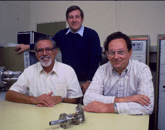
It must be noted
however that as long as in 1966 Russell Young has stated idea about an
opportunity of surface topografing with usage of current between surface and
sharp metallic tip. In 1971 he have published paper about device colled
Topografiner, which contained all major assemblies of Scanning Probe
Microscope.
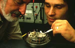
Russell Young and his co-workers Fredric
Scire and John Ward (left to right) with the
Topografiner.
Russel Young
Russell D. Young obtained his B.S. degree in physics
from the Rensselaer Polytechnic Institute in 1953 and his
Ph.D. degree in physics from Pennsylvania State University in
1959. He remained at Penn State in the laboratory of Professor
Erwin Mueller for his postdoctoral research, which was marked
by several outstanding achievements. Among these were the
development of a high resolution field emission energy
analyzer and the first measurement of the total energy
distribution of field emitted electrons, as well as
contributions to the development of the low temperature field
ion microscope. He came to the National Bureau of Standards in
1961. His development of the Topografiner
was an outgrowth of his continued study of surfaces at NBS.
After the termination of this project in 1971, he remained at
NBS in both a technical and an administrative role until his
retirement in 1981. Since then he has actively pursued his
interests as an inventor, as a private consultant to industry
and government (including NIST), and as a grandfather and a
sailor.
Dr. Young's achievements have been
recognized in several awards. In 1974, he was the first
recipient of the Edward U. Condon Award, conferred by NBS in
recognition of outstanding scientific writing. He received the
U.S. Department of Commerce Silver Medal in 1979, a
Presidential Citation in 1986, and the Scientific Achievement
Award of the Washington Academy of Sciences in 1987. In 1992,
the American Vacuum Society recognized his invention of the
Topografiner by presenting him with the Gaede-Langmuir Award.
Description
of Topografiner was published in papers ( Phys. Rev. Lett. V. 27, N
14, 1971, P. 922-924. Full
text.) ( Rev. Sc.
Instr. V. 43, N 7,1972, P. 999-1011. Full text.) , from where presented below figures
and commentaries are taked .
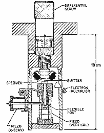 |
Present realization of the Topografiner. The
differential screw is used as a coarse adjustment to bring the
specimen close enough to the emitter so that it is within the
range of the vertical (Z) piezo. The X-scan piezo deflects the
emitter support post so as to scan the emitter in one
direction. The orthogonal (Y) piezo is not shown. The specimen
is clamped between copper blocks to permit heating. An
electron multiplier permits detection of secondary electrons. |
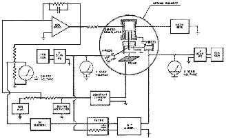
|
Block diagram for the Topografiner electrical
circuitry. The X-Y recorder is frequently replaced with a
memory oscilloscope which results in rapid scan rates with
somewhat reduced fidelily. The OPS bias permits positioning
the emitter at an appropriate distance from the surface.
Details of the servo loop are discussed in the
next. |
|
|
(a)
|
(b)
|
|
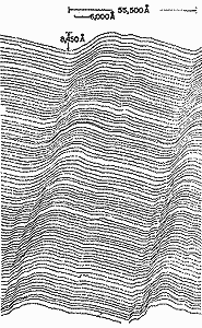
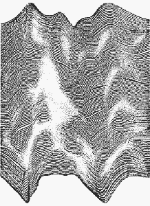
(a) Topographic map of a 180 line/mm diffraction
grating replica. This map was made with using an X-Y recorder.
Note the rippled surface at the base of the groove which may
have been caused by ruling instrument chatter or replica re-
moval. Details of the diamond tool used in the ruling engine
are evident. The emitter was kept about 200 A. above the
surface during these runs.
|
|
|
(b) Topographic map recorded on a memory oscilloscope
of a disturbed region of the same grating as (a). The vertical
magnification is about twice ihe horizontal magnifcation. The
contrast is reversed for easy comparison with (a). The close
spaced prohles give a highly desirable pictorial
representation of the surface topography. Mapping time—9
min.
|
|
|
Though Young has achieved 3 А resolution on Topographiner and pointed out the
opportunity taking images of monoatomic steps, he not assumpted that it is
possible to view single atoms. It was done by Binnig and Rohrer - and they
became Nobelists.
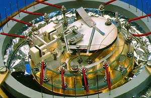
Exact
copy of first Scanning Tunneling Microscope of Binning and Rohrer (original have
not preserved). The photo is kindly submitted for a museum by mister G.
Binnig.
|
|

|
1982.
Triumph of Scanning Probe Microscopy - image of silicon surface 7x7
reconstruction.
|
up
|